Development of an Innovative UV Laser Debonding Process for Advanced Microelectronic Packaging
Overview
- RESEARCH DIRECTION
- Dominique Drouin, Professeur - Department of Electrical and Computer Engineering
- RESEARCH CO-DIRECTION
- Serge Ecoffey, Professeur sous octroi de recherche - Department of Electrical and Computer Engineering
- ADMINISTRATIVE UNIT(S)
-
Faculté de génie
Département de génie chimique et de génie biotechnologique
Département de génie mécanique
Institut interdisciplinaire d'innovation technologique (3IT)
- LEVEL(S)
- 2e cycle
- LOCATION(S)
-
3IT - Institut interdisciplinaire d'innovation technologique
C2MI - Centre de Collaboration MiQro Innovation
Project Description
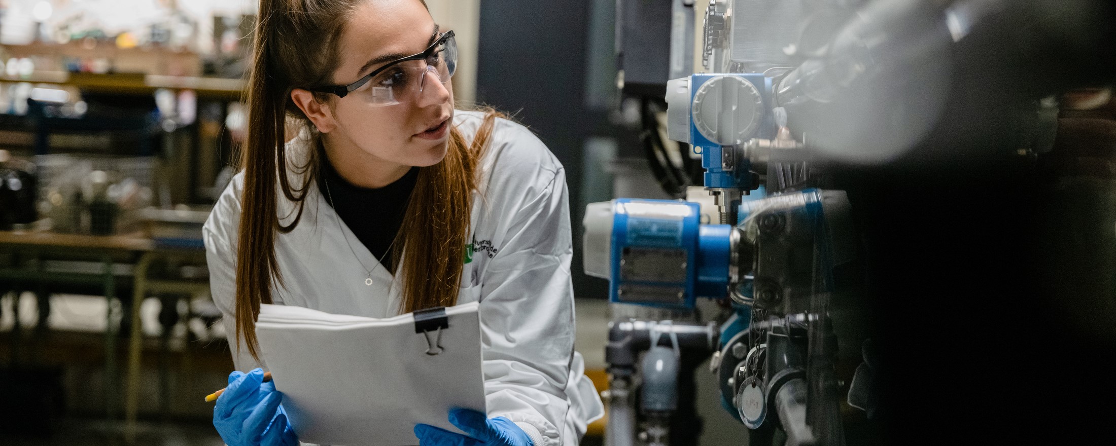
Context:
Advanced packaging technologies are at the heart of modern microelectronic evolution, playing a critical role in meeting the growing demands of artificial intelligence, aerospace, and high performance computing. Among these technologies, Fan Out Wafer Level Packaging (FOWLP) stands out for its ability to deliver high interconnection density and exceptional space efficiency, paving the way for more compact, high performance, and heterogeneous systems.
At the core of these architectures, temporary bonding/debonding (TBDB) processes play a strategic role in enabling flexible functional integration. However, traditional methods—thermal, mechanical, or chemical debonding—are revealing their limitations: sensitivity to high temperatures, risk of cracking in thinned wafers, and reliance on solvents or costly equipment. Laser debonding is emerging as a promising alternative: cleaner, more precise, and better controlled. By leveraging localized photodecomposition of the bonding material, it enables rapid, room temperature debonding without mechanical stress, opening the door to more reliable TBDB processes compatible with the stringent requirements of advanced packaging.

Topic:
We are seeking a highly motivated and qualified candidate to develop an alternative UV laser debonding process (355 nm). Responsibilities include; (i) conducting a literature review on temporary bonding/debonding (TBD) materials and methods,(ii) selecting 2–3 commercially available anti adhesion release layers, and developing the debonding process by UV laser. The role also involves performing morphological and mechanical characterizations of the temporary carrier to assess TBD process quality and evaluating the integrity of Fan Out Wafer Level Packaging (FOWLP) structures after molding and chip interconnection. Key considerations include EMC surface roughness, planarization, and carrier warpage. The project will be carried out in close collaboration with IBM engineers.

Work Supervision:
This MSc project will be realized under the co-direction of Pr. Dominique Drouin and Pr. Serge Ecoffey, as part of the IBM/NSERC Alliance Project on Multi-Chip Heterogeneous Integration for High Performance Computing. The work will be done mainly at the Interdisciplinary Institute for Technological Innovation (3IT) at the Université de Sherbrooke and at the MiQro Innovation Collaborative Center (C2MI) in Bromont. 3IT is a unique institute in Canada, specializing in the research and development of innovative technologies for energy, electronics, robotics and health. C2MI is an international center for collaboration and innovation in the MEMS and encapsulation field. It is the essential link between applied research and the marketing of microelectronics products. The student will thus benefit from an exceptional research environment that combines students, professionals, professors and industrialists working hand-in-hand to develop the technologies of the future.

Desired Profile:
• Bachelor’s degree in mechanical engineering, chemical engineering, or materials science
• Knowledge of materials morphological and mechanical characterization techniques
• Ability to communicate effectively in English or French, both orally and in writing
• Strong adaptability, autonomy, and teamwork skills
• Strong interest in design, experimental work in a cleanroom environment, and research and development
• Assets: Knowledge of integration processes and advanced microelectronic packaging

Contact: inpaqt@usherbrooke.ca

Starting date: september 2026
Documents to provide: Cover letter, curriculum vitae and contact details of 2 references
Discipline(s) by sector
Sciences naturelles et génie
Génie chimique, Génie mécanique
Funding offered
Yes
Partner(s)
IBM Bromont
The last update was on 22 June 2026. The University reserves the right to modify its projects without notice.