Optimization of Micropillar Microfabrication Process for Fan-Out Wafer Level Packaging (FOWLP)
Overview
- RESEARCH DIRECTION
- Dominique Drouin, Professeur - Department of Electrical and Computer Engineering
- ADMINISTRATIVE UNIT(S)
-
Faculté de génie
Département de génie chimique et de génie biotechnologique
Département de génie électrique et de génie informatique
Département de génie mécanique
Institut interdisciplinaire d'innovation technologique (3IT)
- LEVEL(S)
- 3e cycle
- LOCATION(S)
- 3IT - Institut interdisciplinaire d'innovation technologique
Project Description
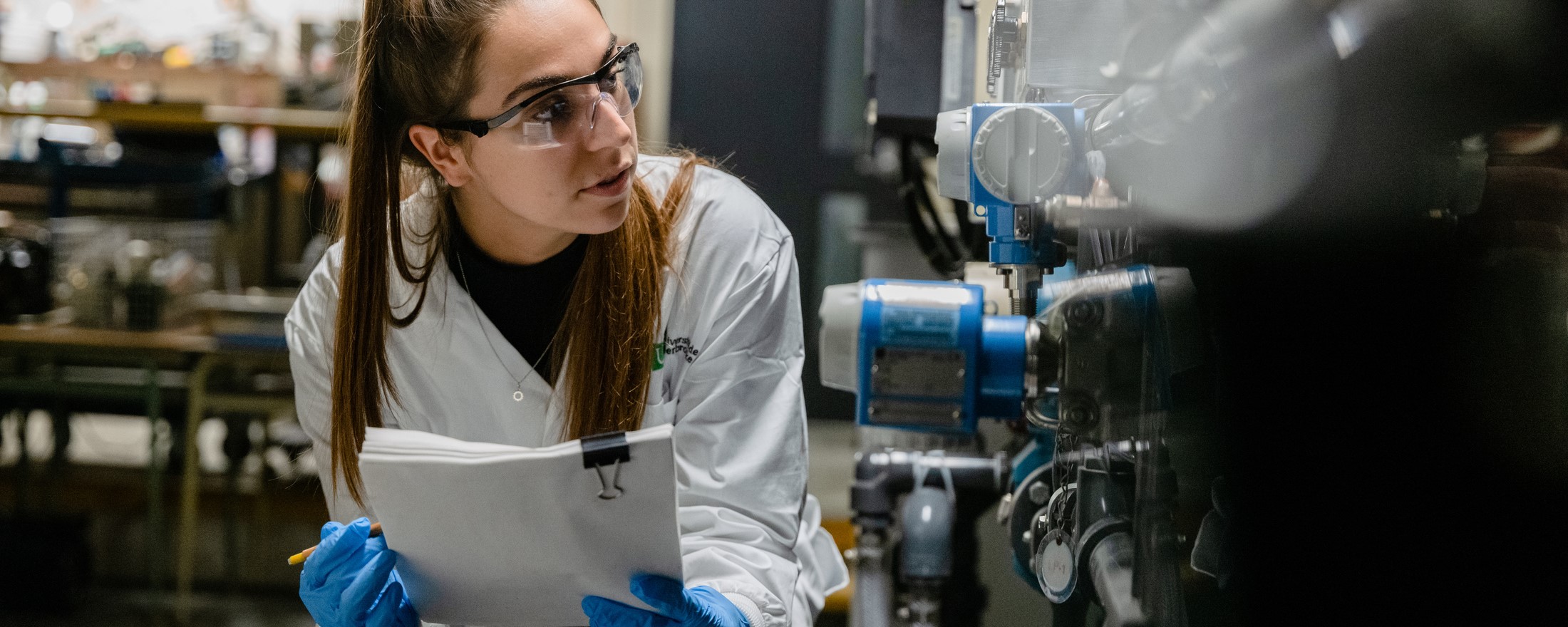
Context:
Advanced packaging technologies are essential for the evolution of microelectronics, enhancing performance through heterogeneous integration. Traditional methods struggle to meet the demands of high-performance computing, AI, aerospace, and defense. With the growing demand for multi-chip heterogenous integration using advanced FOWLP, there is significant interest in reducing the die-to-wafer interconnect pitch, as a smaller pitch enables simpler, more efficient circuits, resulting in lower power consumption and reduced design complexity. However, reducing the bump size to such a pitch introduces new challenges, particularly in terms of thermomechanical strength, resistance to electromigration, and warpage control. In addition, a major challenge in multi-chip FOWLP processes is achieving high-accuracy die placement during the flip-chip die-to-wafer (D2W) bonding process, as the positions of the micro-bumps (contact-pad) must align with the redistribution layer (RDL) masks. This thesis project aims to develop high-density vertical interconnections (< 30 μm pitch) compatible with a manufacturing D2W assembly environment for heterogeneous multichip integration.

Topic:
This thesis aims to engineer an advanced manufacturing process for creating fine-pitch, ductile heterogeneous solder micro-bumps, critical for flip-chip D2W assembly of active chips onto reconstructed wafers. The successful candidate will responsible for: (i) conducting a literature review on microbump fabrication, specifically focusing on the requirements for producing ultra-fine pitch Cu/Ag/Sn micropillars; (ii) optimizing  microfabrication processes to define patterns of micropillars in the clean room, including precise lithography, alignment and exposure techniques; (iii) optimizing the electroplating parameters to create fine-pitch micropillars; (iv) developing thermocompression bonding (TCB-D2W) process conditions (pressure, and head and substrate temperatures) tailored to the unique structure of the micropillars; (v) performing comprehensive morphological characterizations to measure and analyze the uniformity and quality of the micropillars across different sections of the wafers. At the end of this thesis, the student will have established a new compliant interconnect that enhances the integrity of advanced microelectronic systems.

Work Supervision:
This PhD thesis will be realized under the direction of Professor Dominique Drouin, as part of the IBM/NSERC Alliance Project on Multi-Chip Heterogeneous Integration for High-Performance Computing. The work will be conducted primarily at the Interdisciplinary Institute for Technological Innovation (3IT) at the Université de Sherbrooke and at the MiQro Innovation Collaborative Center (C2MI) in Bromont. 3IT is a unique institute in Canada, specializing in the research and development of innovative technologies for energy, electronics, robotics and health. C2MI is an international center for collaboration and innovation in the MEMS and encapsulation field. It is the essential link between applied research and the marketing of microelectronics products. The student will thus benefit from an exceptional research environment that brings together students, professionals, professors and industry professionals working hand-in-hand to develop the technologies of the future.

Desired Profile:
• Master’s degree in micro-nanotechnologies or materials science.
• Skills in clean room microfabrication and electrical characterizations.
• Ability to communicate effectively in English or French, both orally and in writing.
• Strong capacity for adaptation, autonomy and teamwork.
• Pronounced taste for design, experimental work in a clean room, research, and development.
• Assets: Knowledge of integration processes, and advanced microelectronic packaging.

Contact: inpaqt@usherbrooke.ca
Desired starting date: September 2025
Documents to provide: Cover letter, curriculum vitae, transcripts for the past two years, and contact information for 2 references.
Discipline(s) by sector
Sciences naturelles et génie
Génie chimique, Génie électrique et génie électronique, Génie mécanique
Funding offered
Yes
$ 25 000 CAD per year
Partner(s)
IBM Canada Ltée., Institut Interdisciplinaire d’Innovation Technologique (3IT), Centre de Collaboration MiQro Innovation (C2MI)
The last update was on 24 October 2025. The University reserves the right to modify its projects without notice.