AML Wafer Bonder
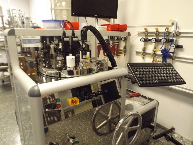
Description
Assembly of substrates or samples by direct, anodic, eutectic or polymeric bonding
Manufacturer and model
Applied Microengineering Ltd - AWB-04
Technical specifications
- Small samples and 100mm substrates
- Clamping of samples of 1cm x 1cm, 75mm and 100mm
- Visible and IR alignment for substrates of 75mm and 100mm
- Assembly under atmosphere and vacuum (~ 0.1mTorr)
- Independent heating of platen up to 500°C
- Anodic bonding up to 2.5kV limited current
- Activation by O₂ plasma
- Minimum assembly force of 150N
- Maximum assembly force of 25kN
- Water vapor injection
Examples of available processes
- Direct Si / Si bonding with plasma activation
- Anodic bonding of Pyrex substrates