PECVD reactors
The 3IT.Nano platform has two PECVD reactors
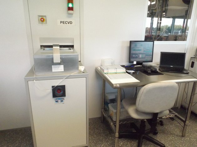
PECVD #1
Description
Deposition of silicon oxide, silicon nitride, silicon oxynitride, silicon carbide, silicon oxycarbide and amorphous silicon. Possibility of phosphorus, boron or german doping.
Manufacturer & model
STS - MESC Multiplex
Technical specifications
- Deposition temperature: from 20°C to 380°C
- Frequencies: 13.56 MHz or 380 kHz; Possibility of using a mixed frequency mode
- Maximum power: 1 kW @ 380 kHz, 300 W @ 13.56 MHz
- Gases installed on the system: NH₃, Ar, N₂, B₂H₆ (diluted to 10% in H₂), GeH₄, CH₄, O₂, PH₃ (diluted to 10% in Ar), N₂O, SiH₄,
- Sample size: substrates up to 200 mm in diameter; compatible with small samples
Examples of available processes
- Deposition of insulating layers for the production of transistor grids
- Deposition for the manufacture of implantation or engraving masks
- Deposition of doped SiO₂ for the manufacture of waveguides
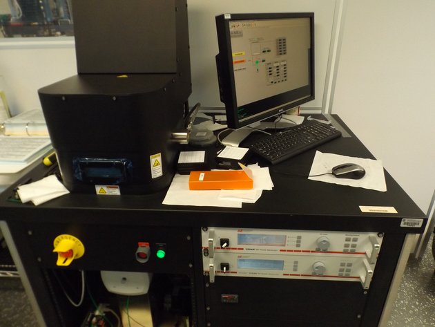
PECVD #2
Description
The PECVD BenchMark is a plasma assisted thin film deposition system. It is mainly used for depositing thin layers of silicon oxide and nitride less than one micrometer thick.
Manufacturer & model
BenchMark - 800-II
Technical specifications
- Samples or substrate deposition up to 200mm (8in) in diameter
- Software interface for process editing and control
Examples of processes available
- Silicon nitride (SiNxHz)
- Silicon oxide (SiOx)