Maxime Darnon
Professeur associé, Faculté de génie
FAC. GÉNIE Électrique et informatique
Présentation
Sujet de recherche
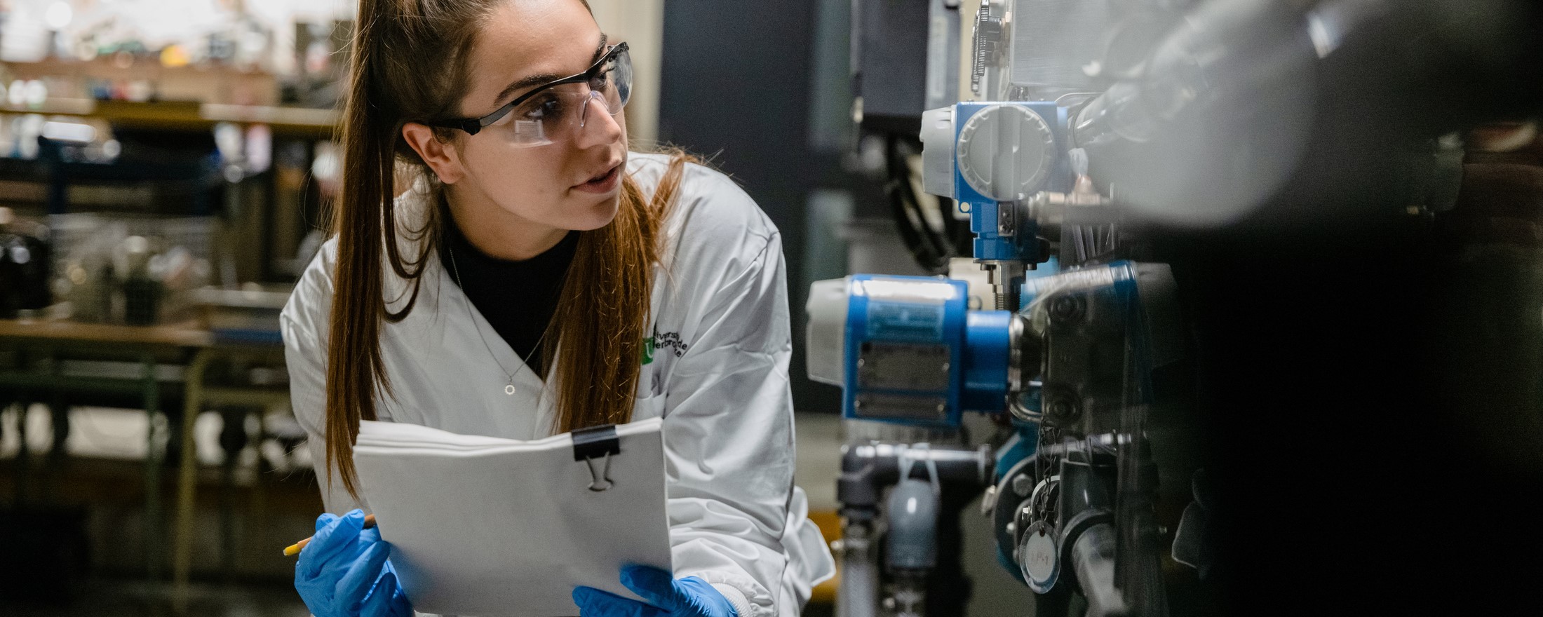
Énergie éolienne et solaire, Micro et nanoélectronique
Disciplines de recherche
Génie électrique et génie électronique
Mots-clés
gravure plasma, micro et nano électronique
Recherche clinique
Langues parlées et écrites
Anglais, Français
Diplômes
(2004). (Equivalent à la maîtrise, ). Institut national polytechnique de Grenoble.
(). (Doctorat, ). Université de Grenoble I - Joseph Fourier.
Prix et distinctions
- (2013) CNRS internal promotion from Class 2 to Class 1 researcher. (Distinction).
- (2010) SEMI Best Young Engineer Award. (Prix / Récompense).
- Habilitation to supervise students (French Diploma Habilitation à Diriger les Recherches). Université de Grenoble I - Joseph Fourier. (Distinction).
Publications
Articles de revue
- G. Cunge, M. Darnon, J. Dubois*, P. Bezard*, O. Mourey*, C. Petit-Etienne, L. Vallier, E. Despiau-Pujo, N. Sadeghi,. (2016). Measuring ion velocity distribution functionsthrough high-aspect ratio holes in inductively coupled plasmas. Applied Physics Letters 108 093109. (Article publié).
- O. Mourey*, C. Petit-Etienne, G. Cunge, M. Darnon, E. Despiau-Pujo, P. Brichon*, E. Lattu-Romain*, M. Pons, O. Joubert. (2016). Roughness generation during Si etching in Cl2 pulsed plasma. Journal of Vacuum Science and Technology A 34 041306. (Article publié).
- B. Lee Sang*, M.-J. Gour, M. Darnon,S. Ecoffey, A. Jaouad, B. Sadani*, D. Drouin, A. Souifi,. (2016). Selective dry etching of TiN nanostructures over SiO2nanotrenches using a Cl2/Ar/N2 inductively coupled plasma. J. Vac. Sci. Technol. B 34 02M102. (Article publié).
- M. Darnon, M. de Lafontaine*, M. Volatier*, S. Fafard, R. Arès, A. Jaouad, V. Aimez. (2015). Deep germanium etching using time multiplexed plasmaetching. J. Vac. Sci; Technol. B 33 060605. (Article publié).
- Lee Sang* B, Gour M-J, Jaouad A, Ecoffey S, Darnon M, Sadani* B, Souifi A, Drouin D. (2015). Inductively coupled plasma etching of ultra-shallowSi3N4 nanostructures using SF6/C4F8chemistry. Microelectron. Eng. 141 68-71. (Article publié).
- M. Darnon, N. Rochat, C. Licitra. (2015). Modification of Porous SiOCH by First Contact withWater Vapor after Plasma Process. J. Vac. Sci. Technol. B 33 (6), 061205. (Article publié).
- Haass* M, Darnon M, Cunge G, Joubert O, Gahan D. (2015). Silicon etching in a pulsed HBr/O2plasma. I. Ion flux and energy analysis. J. Vac. Sci. Technol. B 33 032202. (Article publié).
- Haass* M, Darnon M, Cunge M, Joubert O. (2015). Silicon etching in a pulsed HBr/O2plasma. II. Pattern transfer. J. Vac. Sci. Technol. B 33 032203. (Article publié).
- Lionti* K, Darnon M, Volksen W, Magbitang T, Dubois G. (2015). The efficacy of post porosity plasma protectionagainst vacuum-ultraviolet damage in porous low-k materials. J. Appl. Phys. 117 (11), 113303. (Article publié).
- Lionti* K, Volksen W, Magbitang T, Darnon M, Dubois G. (2015). Toward Successful Integration of Porous Low-kMaterials: Strategies Addressing Plasma Damage. ECS J. Solid State Sci. Technol. 4 (1), N3071-N3083. (Article publié).
- Blanc R, Leverd F, Darnon M, Cunge G, David S, Joubert O. (2014). Patterning of silicon nitride for CMOS gate spacer technology.III. Investigation of synchronously pulsed CH3F/O2/Heplasmas. J. Vac. Sci. Technol. B 32 (2), 021807. (Article publié).
- Ducoté* J, Possémé N, David T, Darnon M, Chevolleau T, Guillermet M. (2014). Prediction of porous dielectric line wigglingphenomenon with metallic hard mask: From simulation to experiment. Appl. Phys. Lett. 104 231603. (Article publié).
- Despiau-Pujo E, Brihoum* M, Bodart* P, Darnon M, Cunge G. (2014). Pulsed Cl2/Ar inductively coupled plasmaprocessing: 0D model versus experiments. Journal of Physics D: Applied Physics 47 (45), 455201-455212. (Article publié).
- Darnon M, Cunge G, St J Braithwaite N. (2014). Time-resolved ion flux, electron temperature andplasma density measurements in a pulsed Ar plasma using a capacitively coupledplanar probe. Plasma Sources Sci. Technol. 23 025002. (Article publié).
- Darnon M, Chevolleau T, Licitra C, Rochat N, Zocco* J. (2013). Analysis of water adsorption in plasma-damaged porous low-k dielectric by controlled-atmosphere infrared spectroscopy. Journal of Vacuum Science \& Technology B 31 (6), 061206. (Article publié).
- Petit-Etienne C, Darnon M, Bodart* P, Fouchier* M, Cunge G, Pargon E, Vallier L, Joubert O, Banna S. (2013). Atomic-scale silicon etching control using pulsed Cl2 plasma. Journal of Vacuum Science \& Technology B 31 (1), 011201. (Article publié).
- Darnon M, Casiez* N, Chevolleau T, Dubois G, Volksen W, Frot* T, Hurand* R, David T, Posseme N, Rochat N, et al. (2013). Impact of low-k structure and porosity on etch processes. J. Vac. Sci. Technol. B 31 011207. (Article publié).
- Bruce RL, Engelmann S, Purushothaman S, Volksen W, Frot* TJ, Magbitang T, Dubois G, Darnon M. (2013). Investigation of plasma etch damage to porous oxycarbosilane ultra low-k dielectric. Journal of Physics D: Applied Physics 46 (26), 265303. (Article publié).
- Brihoum* M, Cunge G, Darnon M, Gahan D, Joubert O, St J Braithwaite N. (2013). Ion flux and ion distribution function measurements in synchronously pulsed inductively coupled plasmas. Journal of Vacuum Science \& Technology A 31 (2), 020604. (Article publié).
- Volksen W, Purushothaman S, Darnon M, Lofaro M, Cohen S, Doyle J, Fuller N, Magbitang T, Rice P, Krupp L, et al. (2012). Integration of a manufacturing grade, k= 2.0 spin-on material in a single damascene structure. ECS Journal of Solid State Science and Technology 1 (5), N85--N90. (Article publié).
- Banna S, Agarwal A, Cunge G, Darnon M, Pargon E, Joubert O. (2012). Pulsed high-density plasmas for advanced dry etching processes. Journal of Vacuum Science \& Technology A 30 (4), 040801. (Article publié).
- Haass* M, Darnon M, Joubert O. (2012). Sidewall passivation layer thickness and composition profiles of etched silicon patterns from angle resolved x-ray photoelectron spectroscopy analysis. Journal of Applied Physics 111 (12), 124905. (Article publié).
- Petit-Etienne C, Pargon E, David S, Darnon M, Vallier L, Joubert O, Banna S. (2012). Silicon recess minimization during gate patterning using synchronous plasma pulsing. Journal of Vacuum Science \& Technology B 30 (4), 040604. (Article publié).
- Licitra C, Chevolleau T, Bouyssou R, El Kodadi M, Haberfehlner G, Hazart J, Virot L, Besacier M, Posseme N, Darnon M, et al. (2011). Development of porosimetry techniques for the characterization of plasma-treated porous ultra low-k materials. ECS Transactions 35 (4), 729--746. (Article publié).
- Petit-Etienne C, Darnon M, Vallier L, Pargon E, Cunge G, Fouchier* M, Bodart* P, Haass* M, Brihoum* M, Joubert O et al. (2011). Etching mechanisms of thin SiO2 exposed to Cl2 plasma. Journal of Vacuum Science \& Technology B 29 (5), 051202. (Article publié).
- Posseme N, Bouyssou* R, Chevolleau T, David T, Arnal V, Darnon M, Brun Ph, Verove C, Joubert O. (2011). Residue growth on metallic hard mask after dielectric etching in fluorocarbon based plasmas. II. Solutions. Journal of Vacuum Science \& Technology B 29 (1), 011018. (Article publié).
- Posseme N, David T, Chevolleau T, Darnon M, Bailly F, Bouyssou* R, Ducote* J, Chaabouni* H, El Kodadi* M, Licitra C et al. (2011). Study of porous SiOCH patterning using metallic hard mask: challenges and solutions. ECS Transactions 35 (4), 667--685. (Article publié).
- Darnon M, Chevolleau T, David T, Ducote* J, Posseme N, Bouyssou* R, Bailly F, Perret D, Joubert O. (2010). Patterning of porous SiOCH using an organic mask: Comparison with a metallic masking strategy. Journal of Vacuum Science \& Technology B 28 (1), 149--156. (Article publié).
- Petit-Etienne C, Darnon M, Vallier L, Pargon E, Cunge G, Boulard* F, Joubert O, Banna S, Lill T. (2010). Reducing damage to Si substrates during gate etching processes by synchronous plasma pulsing. Journal of Vacuum Science \& Technology B 28 (5), 926--934. (Article publié).
- Bailly F, David T, Chevolleau T, Darnon M, Posseme N, Bouyssou* R, Ducote* J, Joubert O, Cardinaud C. (2010). Roughening of porous SiCOH materials in fluorocarbon plasmas. Journal of Applied Physics 108 (1), 014906. (Article publié).
- Darnon M, Petit-Etienne , Pargon E, Cunge G, Vallier L, Bodart* P, Haass* M, Banna S, Lill T, Joubert O. (2010). Synchronous Pulsed Plasma for Silicon Etch Applications. ECS Transactions 27 (1), 717--723. (Article publié).
- Demuynck S, Kim H, Huffman C, Darnon M, Struyf H, Versluijs J, Claes M, Vereecke G, Verdonck P, Volders H, et al. (2009). Dielectric Reliability of 50 nm Half Pitch Structures in Aurora LK. Japanese Journal of Applied Physics 48 (4S), 04C018. (Article publié).
- Guillorn M, Chang J, Fuller N, Patel J, Darnon M, Pyzyna A, Joseph E, Engelmann S, Ott J, Newbury J, et al. (2009). Hydrogen silsesquioxane-based hybrid electron beam and optical lithography for high density circuit prototyping. Journal of Vacuum Science \& Technology B 27 (6), 2588--2592. (Article publié).
Livres
- Posseme N, Darnon M, Chevolleau T, David T. (2015). Plasma Etching Processes for Interconnect Realization in VLSI. Elsevier. (Article publié).
Articles de conférence
- M. Darnon, A. Jaouad, M. de Lafontaine*, C. Colin*, O. Richard*, B. Bouzazi*, M. Volatier*, R. Ares, S. Fafard, V. Aimez. (2016). IEEE Photonics North (PN),QuébecMicrotechnologies for high efficiency solar cells, , , doi: 10.1109/PN.2016.7537907. IEEE, (Article publié).
- M. de Lafontaine*, M. Darnon, A. Jaouad, P. Albert*, B. Bouzazi*, C. Colin*, M. Volatier*, S. Fafard, R. Arès, V. Aimez,. (2016). Plasmaetching applications in concentrated photovoltaic cell fabrication. AIP Proceedings, 060001. (Article publié).
- Renaud Varache*, Maxime Darnon , Médéric Descazeaux*, Mickael Martin, Thierry Baron, Delfina Muñoz. (2015). Evolutionof bulk c-Si properties during the processing of GaP/c-Si heterojunction cell. Energy Procedia, 493-499. (Article publié).
- M. Darnon, R. Varache*, M. Descazeaux*, T. Quinci*, M. Martin, T. Baron, D. Muñoz. (2015). Solar cells with gallium phosphide/silicon heterojunction. AIP Conference Proceedings, 060003. (Article publié).
- Dupuy E, Pargon E, Fouchier M, Grampeix H, Pradelles J, Darnon M, Pimenta-Barros P, Barnola S, Joubert O. (2015). Spectral analysis of the linewidth and line edgeroughness transfer during a self-aligned double patterning process. Proc. SPIE 94258, Advanced Etch Technology for Nanopatterning II, 94280B. (Article publié).
- O. Richard*, M. Volatier*, M. Darnon, A. Jaouad, B. Bouzazi*, R. Arès, S. Fafard, V. Aimez. (2015). Throughcell vias contacts for multijunction solar cells. AIP Conference Proceedings, 060003. (Article publié).
- Darnon M, Posseme N, Chevolleau T, David T. (2014). Prospectsfor dielectric constant reduction in integrated circuits interconnects. Proceeding of the 2014 MRS Spring Meeting, 162. (Article publié).
- Darnon M, Haass* M, Cunge G, Joubert O, Banna S. (2013). Characterization of silicon etching in synchronized pulsed plasma. Proc. SPIE 8685, Advanced Etch Technology for Nanopatterning II, 86850J-. (Article publié).
- Chevolleau T, Cunge G, Delalande* M, Chevalier X, Tiron R, David S, Darnon M, Navarro C. (2012). Self-assembly patterning using block copolymer for advanced CMOS technology: optimisation of plasma etching process. Proceedings of the SPIE - The International Society for Optical Engineering, 83280M. (Article publié).
- Joubert O, Darnon M, Cunge G, Pargon E, David T, Petit-Etienne C, Vallier L, Posseme N, Bodart* P, Azarnouche* L et al. (2012). Towards new plasma technologies for 22nm gate etch processes and beyond. Proceedings of the SPIE - The International Society for Optical Engineering, 83280D. (Article publié).
- Darnon M, Chevolleau T,David T, Posseme N, Bouyssou* R, Hurand* R, Joubert O, Licitra C, Rochat N, Bailly F, Verove C. (2011). Impactof ambient atmosphere on plasma-damaged porous low-k characterization. IEEE International, 5940348. (Article publié).
- Hurand* R, Bouyssou* R, Darnon M, Tiphine* C, Licitra C, El-kodadi* M, Chevolleau T, David T, Posseme N, Besacier M, Schiavone P, Bailly F, Joubert O, Verove C. (2011). Scatterometric Porosimetry for porous low-k patterns characterization. IEEE International, 5940350. (Article publié).
- Chevolleau T, Posseme N, David T, Bouyssou* R, Ducote* J, Bailly F, Darnon M, El Kodadi* M, Besacier M, Licitra C et al. (2010). Etching process scalability and challenges for ULK materials. Proceeding of IEEE International Interconnect Technology Conference, 1--3. (Article publié).
- Guillorn M, Chang J, Pyzyna A, Engelmann S, Joseph E, Fletcher* B, Cabral C, Lin CH, Bryant A, Darnon M, Ott J, Lavoie C, Frank M, Gignac L, Newbury J, Wang C, Klaus D, et al. (2009). Trigate6T SRAM scaling to 0.06 μm2. , Proceeding of 2009 International Electron Devices Meeting, (Article publié).
Propriétés intellectuelles
Brevets
- (2015). Embedded test structure for trimming process control. US 8,956,886. États-Unis. (Délivré).
- (2015). Interconnect structures containing a photo-patternable low-k dielectric with a curved sidewall surface. US9,059,249. États-Unis. (Délivré).
- (2015). Methods for fabrication of an air gap-containing interconnect structure. US8,952,539. États-Unis. (Délivré).
- (2015). Multi-level autolimitating etching method. US 9,123,652. France. (Délivré).
- (2014). 5 Methodology for evaluation of electrical characteristics of carbon nanotubes. US 8,828,749. États-Unis. (Délivré).
- (2014). Air gap-containing interconnect structure having photo-patternable low k material,. US 8,629,561. États-Unis. (Délivré).
- (2014). Methodology for evaluation of electrical characteristics of carbon nanotubes. US 8,853,856. États-Unis. (Délivré).
- (2014). Methods for fabrication of an air gap-containing interconnect structure,. US 8,642,252. États-Unis. (Délivré).
- (2014). Methods for photo-patternable low-k (PPLK) integration with curing after pattern transfer. US 8,637,395. États-Unis. (Délivré).
- (2014). Procédé de gravure autolimitant à niveaux multiples. FR 3,002,689. France. (Délivré).
- (2014). Structure and method for air gap interconnect integration. US 8,896,120. États-Unis. (Délivré).
- (2013). Method of patterning of magnetic tunnel junctions. US 8,546,263. États-Unis. (Délivré).
- (2013). Method of patterning photosensitive material on a substrate containing a latent acid generator. US 8,475,667. États-Unis. (Délivré).
- (2013). Selective etch back process for carbon nanotubes integration. US 8,449,781. États-Unis. (Délivré).
- (2012). Interconnect structure fabricated without dry plasma etch processing. US 8,298,937. États-Unis. (Délivré).
- (2012). Method for air gap interconnect integration using photo-patternable low k material. US 8,241,992. États-Unis. (Délivré).
- (2012). Reversing tone of patterns on integrated circuit and nanoscale fabrication,. US 8,183,694. États-Unis. (Délivré).
- (2011). Process for reversing tone of patterning on integrated circuit and structural process for nanoscale fabrication. US 7,939,446. États-Unis. (Délivré).
- (2010). Forming Interconnects with Air Gaps,. US 7,790,601. États-Unis. (Délivré).
- Procédé de fabrication d’un dispositive résistif pour circuit mémoire ou logique. FR20140060073. France. (En instance).
Autres contributions
Gestion d'évènements
- Member of scientific committee. Journées Nationales des Technologies emmergentes en micro et nano fabrication (JNTE). (Conférence).
- Member of scientific and organizing committee. Plasma Etch and Strip in Microelectronics. (Conférence).
- Member of scientific and organizing committee. Plasma Etch and Strip in Microelectronics. (Conférence).
- Member of scientific and organizing committee. Plasma Etch and Strip in Microtechnologies. (Conférence).
Activités de collaboration internationale
- Chercheur. France. A poursuivi des activités de recherche dans la gravure plasma au sein d'un laboratoire CNRS à Grenoble, France.
- Membre d'un laboratoire international. Canada. Poursuis des activités de recherche dans unlaboratoire international entre le CNRS (France) et l’Université de Sherbrooke(Canada) à Sherbrooke.
Présentations
- (2015). Multi-junction Solar Cells with Through Substrate Vias Contacts. Next Generation PhotoVoltaics Canada. Toronto, Canada
- (2015). Porous Materials Characterization by Infrared Spectroscopy. CMOS Emerging Technologies Research. Vancouver, Canada
- (2015). Solar Cell with Gallium Phosphide / Silicon Heterojunction. CMOS Emerging Technologies Research. Vancouver, Canada
- (2014). Optical and electrical diagnostics in chlorine based pulsed plasmas of an industrial silicon etching reactor. 1st International Middle-East Plasma Science. Antalya, Turquie
- (2014). Plasma Damage of Porous Low-k Materials. Material Research Society Spring Meeting. San Francisco, États-Unis
- (2014). Pulsed Plasmas for etching in micro and nanoelectronics. Plasma Nanoscience Conference. Dublin, Irlande
- (2013). Characterization of silicon etching in synchronized pulsed plasma. SPIE-AL. San Jose, États-Unis
- (2013). Optical and Electrical Diagnostics of Pulsed Plasmas Etching Processes. AVS 60h international symposium. Long Beach, États-Unis
- (2013). Optical and Electrical Diagnostics of Pulsed Plasmas Etching Processes. 11th Technological Plasma Workshop. York, Royaume-Uni
- (2013). Pulsed ICP chlorine plasmas : Numerical simulations versus Experiments. 4th Workshop on Radio Frequency Discharges. Giens, France
- (2013). Pulsed ICP plasmas processing : A combined modelling and experimental study. 31st International Conference on Phenomena in Ionized Gases (ICPIG). Granada, Espagne
- (2013). Pulsed plasmas: from plasma parameters to pattern transfer. Plasma Etch and Strip in Microtechnologies conference. Leuven, Belgique
- (2013). Pulsed plasmas for etching at the nanoscale. Journées Nationales des Technologies Emergentes. Evian, France
- (2013). Pulsed plasmas for etching in microelectronics. Journées du réseau plasma froids. La Rochelle, France
- (2012). Challenges related to linewidth roughness. China Semiconductor Technology International Conference (CSTIC) 2012. Shangai, Chine
- (2012). Plasma Etching for Back End Of Line Applications. China Semiconductor Technology International Conference (CSTIC). Shanghai, Chine
- (2012). Plasmas Processes Challenges for Porous SiCOH Integration in Advanced Interconnects. Materials Research Society spring meeting. San Francisco, États-Unis
- (2012). Plasma treatments to improve Linewidth roughness during gate patterning. SPIE-AL. San Jose, États-Unis
- (2012). Self-assembly patterning using block copolymer for advanced CMOS technology: optimisation of plasma etching process. SPIE-AL. San Jose, États-Unis
- (2012). Towards new plasma technologies for 22nm gate etch processes and beyond. SPIE-AL. San Jose, États-Unis
- (2011). 20 Challenges of porous SiCOH dielectric material integration for advanced interconnect technology nodes. CMOS Emerging Technologies. Wistler, Canada
- (2011). Angstrom Level Resolution Etch. China Semiconductor Technology International Conference (CSTIC). Shangai, Chine
- (2011). Challenges of porous SiCOH dielectric material integration for advanced interconnect technology nodes. CMOS Emerging Technologies. Whistler, Canada
- (2011). Characterizing Plasma Induced Damage to Ultra Low-k. China Semiconductor Technology International Conference (CSTIC). Shanghai, Chine
- (2011). Characterizing plasma-damaged porous low-k. 4th Plasma Etch and Strip in Microelectronics. Mechelen, Belgique
- (2011). Development of Porosimetry Techniques for the Characterization of Plasma-Treated Porous Ultra Low-K Materials. 219th electrochem. Soc. Meeting. Montreal, Canada
- (2011). Diagnostics of reactive pulsed plasmas by UV and VUV absorption spectroscopy and by modulated beam Mass spectrometry. IX workshop on frontiers in low temperature plasma diagnostics. Zinowitz, Allemagne
- (2011). Etch processes with pulsed plasmas for advanced CMOS technologies. 3rd International Conference on Microelectronics and Plasma Technology. Dalian, Chine
- (2011). Improving Etch Processes by Using Pulsed Plasmas. AVS 58h international symposium. Nashville, États-Unis
- (2011). Interest of synchronized pulsed plasmas for next CMOS technologies. China Semiconductor Technology International Conference (CSTIC) 2011. Shangai, Chine
- (2011). Low k Integration Using Metallic Hard Masks. Materials Research Society spring meeting (MRS). San Francisco, États-Unis
- (2011). Porous SiCOH Patterning for Advanced Interconnects: Challenges and Solutions. 219th Electrochemical Soc. Meeting,. Montreal, Canada
- (2011). Reduction of Plasma Induced Silicon-Recess During Gate Over-Etch Using Synchronous Pulsed Plasmas. AVS 57th international symposium. Albuquerqu, États-Unis
- (2011). Time-Modulation of High density Plasmas for Advanced Dry Etching Processes. Plasma Etch and Strip in Microelectronics Workshop. Malin, Belgique
- (2011). Time-resolved diagnostics of pulsed plasmas by UV and VUV absorption spectroscopy and by modulated beam Mass spectrometry. 64th Gaseous Electronic Conference. Salt Lake City, États-Unis
- (2010). Plasma Processes Challenges for Porous SiOCH Patterning in Advanced Interconnects. AVS 57th international symposium, Albuquerque, October 2010. Albuquerque, États-Unis
- (2010). Pulsed plasmas for nanoCMOS and nanoelectronics devices elaboration. 2nd International Conference on Plasma Nanoscience (iPlasma Nano-II). Bateman’s Bay, Australie
- (2010). Synchronized pulsed plasmas: potential process improvements for patterning technologies. 63rd Gaseous Electronic Conference and 7th International Conference on Reactive Plasmas. Paris, France
- (2010). Synchronous Plasma Pulsing for Etch Applications. China Semiconductor Technology International Conference (CSTIC). Shanghai, Chine