Julien Sylvestre
Professeur, Faculté de génie
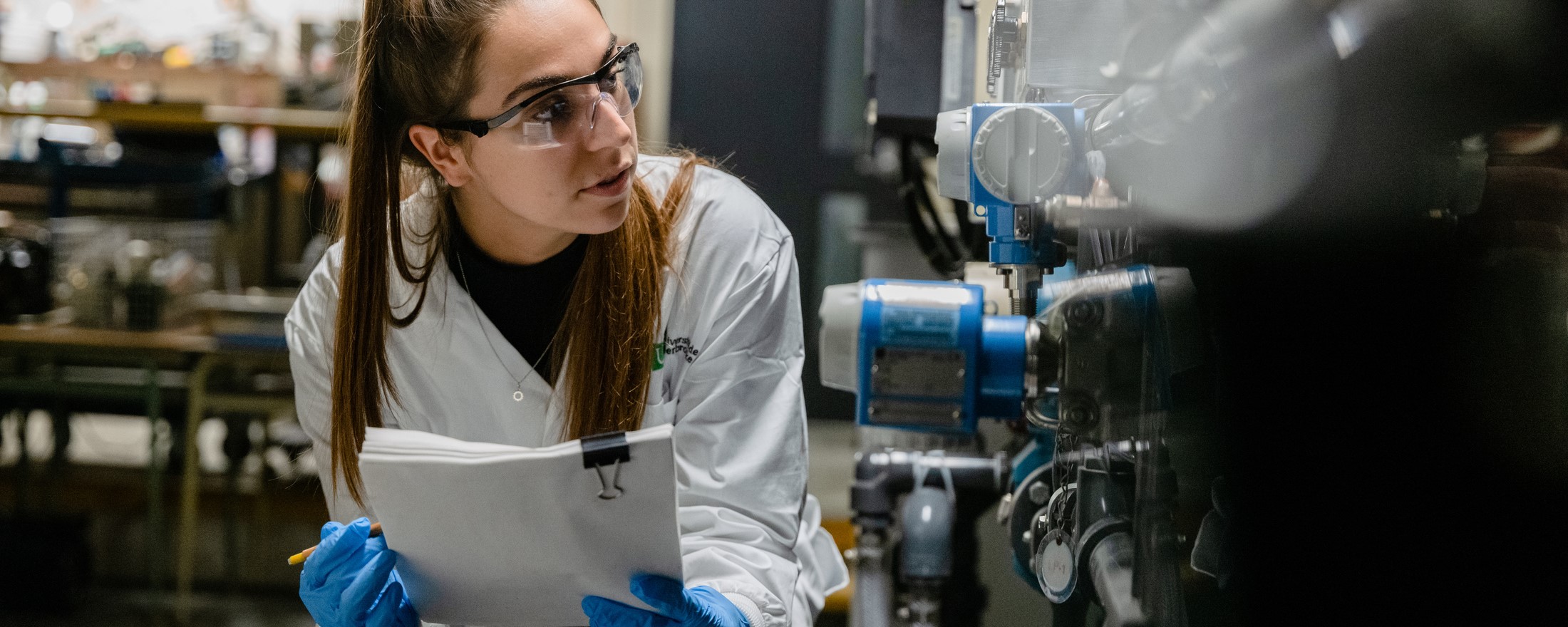
FAC. GÉNIE Mécanique
Présentation
Sujet de recherche
Analyse numérique, Nanosystèmes, Procédés physiques et mécaniques, Analyse des contraintes, Micro et nanoélectronique
Disciplines de recherche
Génie mécanique, Génie des matériaux et génie métallurgique
Mots-clés
Analyse par éléments finis, Dispositifs nanométriques, Encapsulation microélectronique, Procédés industriels en microélectronique, Simulation numérique
Recherche clinique
Langues parlées et écrites
Anglais, Français
Diplômes
(2002). (Doctorat, Philosophiae doctor). Massachusetts Institute of Technology.
(1998). (Baccalauréat avec distinctions, baccalauréat universitaire ès sciences). McGill University.
Publications
Articles de revue
- Sylvestre J, Samson M, Langlois-Demers D, Duchesne E. (2014). Modeling the Flip-Chip Wetting Process. IEEE Transactions on Components, Packaging, and Manufacturing Technology (Article sous presse).
- Sylvestre J. (2011). Vibrations in the Flip-Chip Soldering Process. Components, Packaging and Manufacturing Technology, IEEE Transactions on 1 (6), 904--911. (Article publié).
- Sylvestre J, Blander A. (2008). Large-scale correlations in the orientation of grains in lead-free solder joints. Journal of Electronic Materials 37 (10), 1618--1623. (Article publié).
- Abbott B, Abbott R, Adhikari R, Agresti J, Ajith P, Allen B, Amin R, Anderson S, Anderson W, Arain M, et al. (2008). Search for gravitational waves associated with 39 gamma-ray bursts using data from the second, third, and fourth LIGO runs. Physical Review D 77 (6), 062004. (Article publié).
Articles de conférence
- Sylvestre J, Samson M, Duchesne E, Langlois-Demers D. (2014). LARGE-SCALE MODEL OF FLIP-CHIP JOINING DEFECTS. ASME 2014 International Mechanical Engineering Congress & Exposition. (Article accepté).
- Paquet M, Sylvestre J, Gros E, Boyer N. (2009). Underfill delamination to chip sidewall in advanced flip chip packages. Electronic Components and Technology Conference, 2009. ECTC 2009. 59th, (Article publié).
- Sylvestre M, Blander A, Oberson V, Perfecto E, Srivastava K. (2008). The impact of process parameters on the fracture of device structures during chip joining on organic laminates. Electronic Components and Technology Conference, 2008. ECTC 2008. 58th, (Article publié).
Propriétés intellectuelles
Brevets
- (2014). UNDERFILL ADHESION MEASUREMENTS AT A MICROSCOPIC SCALE. US Patent 8,796,049. (Terminé).
- (2012). Optimization of metallurgical properties of a solder joint. US Patent 8,197,612. (Terminé).
- (2010). Method for measuring thin layers in solid state devices. ZL200710112010.4. (Terminé).
- (2009). Temporary structure to reduce stress and warpage in a flip chip organic package. US Patent 7,538,432. (Terminé).
- (2009). Method for measuring thin layers in solid state devices. US Patent 7,512,518. (Terminé).
- (2009). Structure and method for stress reduction in flip chip microelectronic packages using underfill materials with spatially varying properties. US Patent 7,498,198. (Terminé).
- (2009). Method for determining the impact of layer thicknesses on laminate warpage. US Patent 7,482,180. (Terminé).
- (2009). Method to optimize the manufacturing of interconnects in microelectronic packages. US Patent 7,484,190. (Terminé).
- (2009). Temporary structure to reduce stress and warpage in a flip chip organic package. US Patent 7,473,618. (Terminé).
- ADDITIVES FOR GRAIN FRAGMENTATION IN Pb-FREE Sn-BASED SOLDER. US Patent 8,493,746. (Terminé).
- LOW-STRESS DUAL UNDERFILL PACKAGE. US Patent App.. (Demande en cours).
- METHOD AND APPARATUS TO MINIMIZE STRESS DURING REFLOW PROCESS. US Patent App. 12/127,895. (Demande en cours).
- Methods and Systems Involving Soldering. US Patent App. 13/027,375. (Demande en cours).
- THERMOCOMPRESSION FOR SEMICONDUCTOR CHIP ASSEMBLY. US Patent App.. (Demande en cours).
Divulgations
Autres contributions
Activités de collaboration internationale
- Investigator.
Présentations
- (2014). Large-Scale Model of Flip-Chip Joining Defects. ASME International Mechanical Engineering Congress & Exposition. Montreal
- (2014). Packaging World's Most Advanced Semiconductors: Designing Around Fifty Years of Hard-Learned Lessons. CMC Microsystems Annual Symposium. Gatineau
- (2014). Fiabilité, défauts, fabricabilité: modéliser la complexité des structures encapsulées. Entretiens Jacques-Cartier. Bromont
- (2014). Devil's in the Detail: Large Scale Modeling of Package Manufacturing Defects. CMOS Emerging Technologies Research. Grenoble
- (2008). The impact of process parameters on the fracture of device structures during chip joining on organic laminates. Electronic Components and Technology Conference. Lake Buena Vista