Microtechnologies
Welcome to the world of microtechnology. Discover a platform dedicated to the study of objects on a submillimeter scale.
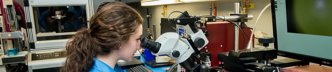
The microtechnology platform (3IT. Micro) brings together equipment and technical expertise for the design, assembly, programming and characterization of advanced prototypes involving expertise in microelectronics (including encapsulation for the integration of nanotechnology devices) and in the domain of telecommunications.
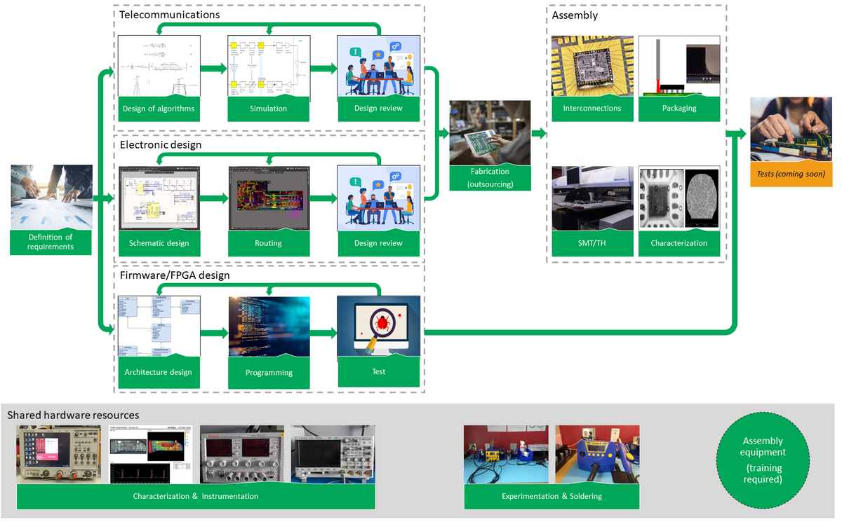
The platform offers a PCB design service. These are designed according to the customer’s electronic and mechanical requirements, from the simplest to the most complex. The design team can also complete an existing design, make a new revision of an existing circuit, or even simply do a design review. Since the platform has a complete assembly line, it is possible to offer turnkey solutions that include the assembly of prototypes.
The platform benefits from cutting edge equipment, allowing the development of chip and PCB assembly processes, chip encapsulation, and surface mount and through-hole assembly processes for the production of physical prototypes. The prototyping service is also offered to SMEs in the region and other academic institutions.
The platform also offers an FPGA/SoC programming and embedded software design service. Whether it is for the design of a specific module of a system or for the complete support of the programming of an embedded system, the resources are committed to developing a solution that corresponds to the needs of the customers. This opportunity is intended for both researchers and companies.
The 3IT.Micro infrastructure offers telecommunications and signal processing design, development and integration services to the entire community of academic researchers or in partnership with businesses. We offer to design the entire flow, from analysis and simulation to hardware implementation. We can also complete an existing design or simply act as a consultant during the design phase of your project. With the available equipment, it is also possible to perform real-time tests (Hardware-in-the-Loop), under various propagation environments.
A characterization and instrumentation laboratory is present in the platform environment. Its mission is to develop electronic circuits for various applications such as medical imaging, microelectronics applied to large experiments in particle physics, neurostimulation/neuronal recording protheses, communication systems and human–electronic interfaces.
- Four stations with computers are available for users of the platform.
- A MT1500 soldering station can be used for reworking printed circuit boards with small components.
- The laboratory is attached to the radiation protection room which allows experiments with radioactivity to be carried out (training form the radiation protection service is required).
An experimentation and soldering laboratory is available to users and provides access to basic test equipment (oscilloscopes, power supplies, waveform generators and others), experimentation areas with computers and a complete soldering station. Wires of various gauges (stranded and solid) are also available on a self-service basis to facilitate assembly and experimentation.
Platform's expertise
Here is an overview of the know-how in microtechnologies, developed thanks to a stable and permanent team of technicians and professionals:
- Chip assembly (wire bonding, flip chip, thermocompression);
- Surface mounted (SMT) and through-hole assembly, on printed circuits boards (single or double sided);
- Lead-free soldering (RoHS);
- Laser cutting and engraving;
- X-ray defect analysis;
- 3D inspection;
- Rework (hot air and infrared);
- Plasma surface treatment;
- Thermal cycling in environmental chamber;
- UV adhesives curing;
- Printed circuit board (PCB) design: multilayer circuits, high density technologies (micro-vias, blind and buried vias), controlled impedance, trace length matching, high frequency differential signals (FPGA, DDR3 memory, etc.), EMI / EMC constraints, substrates (FR4, polyimide, Rogers, silicon, etc.), flex / rigid-flex circuits;
- Silicon interposer design
- FPGA/SoC programming and embedded software design service;
- Equipment rental (oscilloscope, EMI / EMC inspection, etc.);
- Training on equipment accessible in our laboratories;
- Storage (-40°C freezer);
- Telecommunications systems;
- Signal processing algorithms;
- Simulation and test benches;
- FPGA implementation (VHDL/Verilog);
- Hardware-in-the-loop tests.
3IT.Micro presentation
Click on the link below to access a short presentation of the 3IT.Micro plaftorm